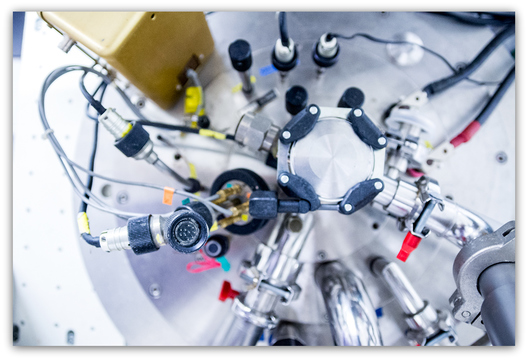
VG Semicon V-80HI
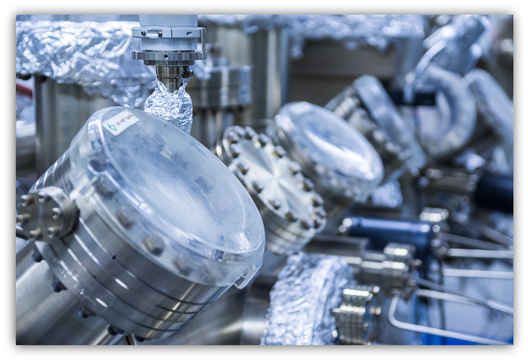
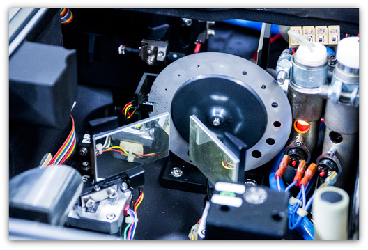
Molecular beam epitaxy (MBE) is one kind of vacuum deposition methods, particularly suited for growing high-quality semiconductor heterostructures with very sharp interfaces and atomic-level thickness precision. In the MBE system, constituent materials of semiconductors, such as gallium, aluminum, and arsenic, are heated in crucibles. The molecular beams of those materials can be switched on and off by mechanical shutters. The crystal growth process takes place in an ultra-high vacuum condition, which is achieved by powerful vacuum pumps (ion pumps, cryopumps, etc.) and liquid N2 shroud. The growth front of the crystals can be monitored in-situ by reflection high energy electron diffraction (RHEED).
VG V80H is used for growing various kinds of heterostructures, including superlattices, self-assembled InAs quantum dots, and various kinds of quantum device structures.
Riber 23
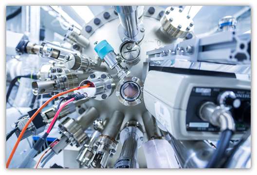
Riber 32p is one of two MBE system in our group. This is equipped with two large cryopumps (CT-10) and is dedicated for growing high-mobility heterostructures. Therefore, the sources in this machine are only Ga, Al, In, As and Si.
Thermal evaporators
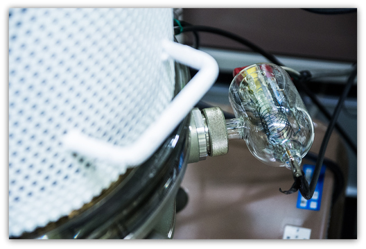
Thermal evaporators are used to deposit metal films by thermal heating. These are equipped with a film thinckness monitor. Therefore, we can deposit metal films with thickness of angstrom levels. We have two evaporators; one for Schottky contacts and the other for Ohmic contacts.
Electron Beam (EB) evaporator
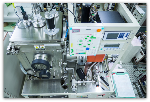
We can evaporate metals such as gold, Cr, and Ti by irradiating the electron beam on such metal targets. This EB evaporator is equipped with a cryopump. Furthermore, this machine is equipped with the substrate tilting system, which can fabricate ultrasmall metal junctions by the shadow evaporation technique.
Atomic layer deposition (ALD) (Cambridge Nanotech)
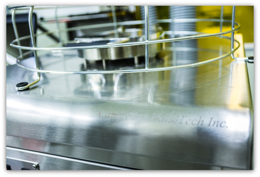
ALD performs layer-by-layer deposition of insulators by alternately supplying precursors. The system can deposit Al2O3 and HfO2 at temperature range from 100~250 °C.
Mask aligner for photolithography (Suss MicroTech)
Standard mask aligner for photolithography. We have various types of sample- and mask-holders to meet demands for various types of sample fabrication.
Atomic force microscope (AFM)
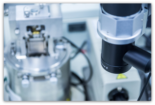
This AFM is used not only for surface characterization of nanostructures but also for patterning by using AFM-assisted anodic oxidation.
Wavelength-tunable femtosecond laser system (Mira 900 f)
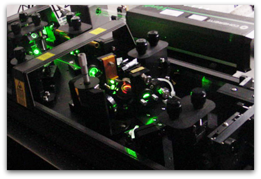
This laser system is used mainly for time-domain terahertz spectroscopy.
Pulse width ~ 100 fs, repetition rate ~ 76 MHz, center wavelength ~ 700-900 nm
Ultra-short pulse femtosecond laser system (Femtolasers)
This laser is used for investigating ultra-fast phenomena in semiconductors or generating ultra-broadband terahertz radiation. Pulse width ~ 10 fs, repetition frequency ~ 75 MHz, center wavelength ~ 800 nm, output power > 300 mW
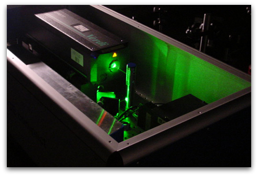
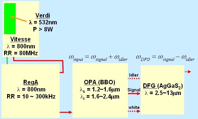
Mid-infrared femtosecond laser system
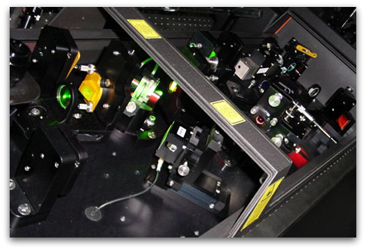
This laser system consists of a femtosecond oscillator, a regeneration amplifier, an OPO, and a AgGaS2 DFG.

Fourier transform infrared spectrometers (FTIR)
We have 2 vacuum-type Fourier transform spectrometers that can cover a very wide frequency range from 10 cm-1 to 15,000 cm-1. Both rapid scan and step scan can be performed.
Far infrared laser (FIR laser)
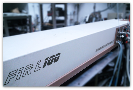
This laser can generate coherent single-frequency far infrared laser lines by using various kinds of molecular gases pumped by a CO2 laser. The commonly used output is a 2.5 THz radiation from CH3OH gas. The maximum output power at 2.5 THz is ~ 100 mW. We use this intense FIR laser beam to induce photon assisted tunneling effects in nanostructures.
Micro-Raman/photoluminescence spectrometer
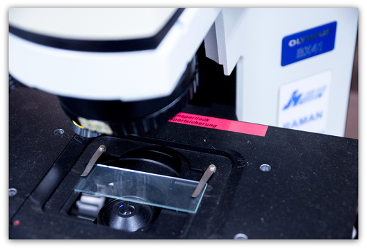
This spectrometer combined with a microscope allows us to take a spatially resolved Raman and photoluminescence spectra of nanostructures.
Superconducting magnet with dilution refrigerator
A dilution refrigerator can cool down samples at temperatures as low as a few tens mK. Magnetic fields up to 15 T can be generated.
Superconducting magnet with an in-situ far infrared detector
A superconducting magnet that accommodates a far infrared detector (1 K bolometer) in the cryostat.